
DirectX ML Shader Model 6.9: How Cooperative Vectors Bring Neural Rendering to HLSL — GDC 2026 Deep Dive
March 24, 2026
AI Streaming Fraud Guilty Plea: How One Man Used Boomy to Generate 661,000 Fake Streams Per Day and Stole $10 Million
March 24, 2026
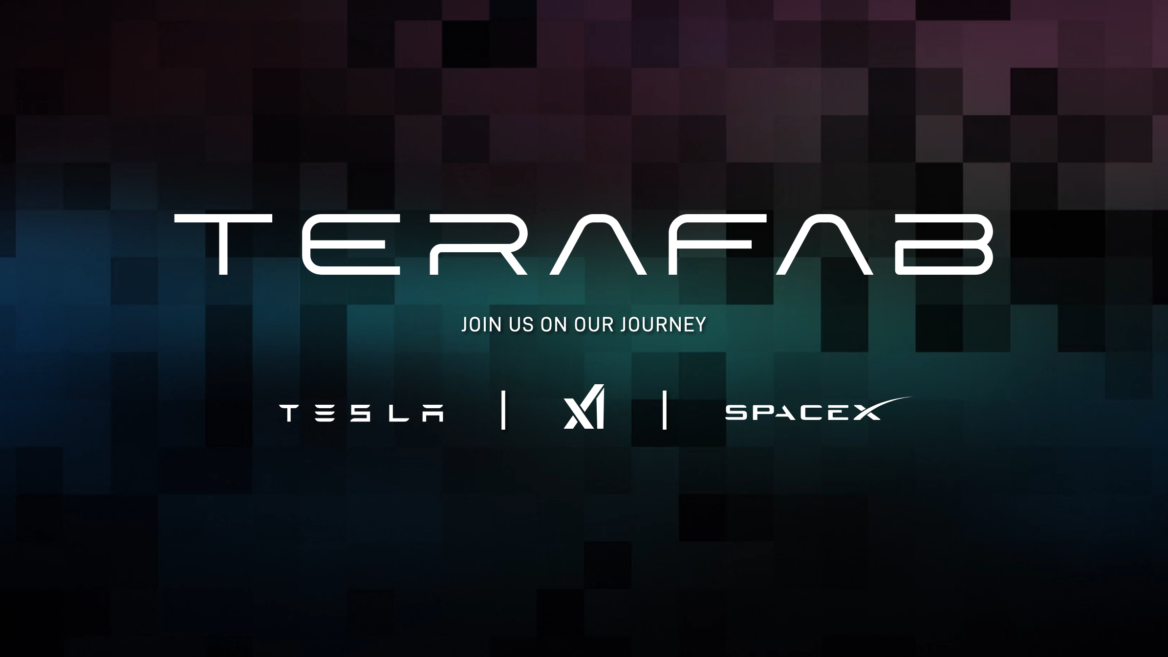
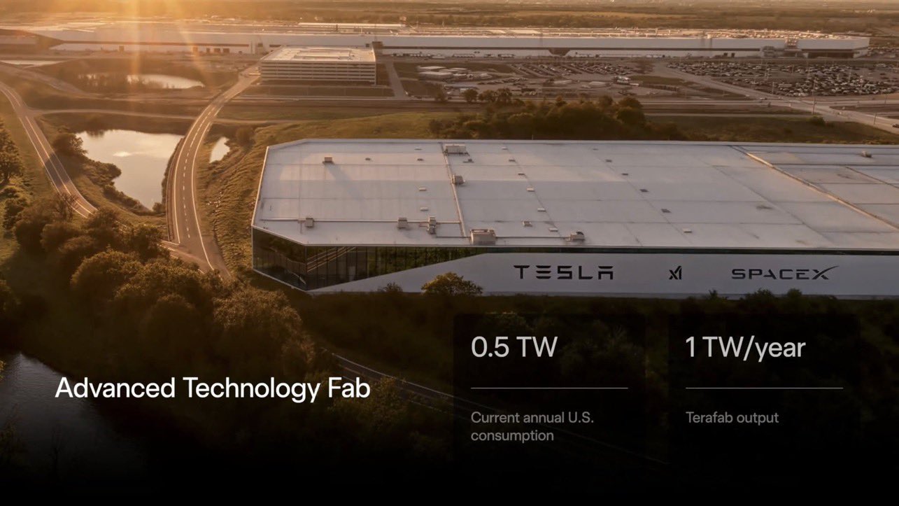
“We either build the Terafab or we don’t have the chips.” That single sentence from Elon Musk on March 21, 2026, announced what could become the most ambitious semiconductor project in history — a $25 billion chip factory designed to produce one terawatt of AI computing power annually. The Terafab chip factory isn’t just another fab; it’s a declaration of war against chip dependency.
What Is the Terafab Chip Factory?
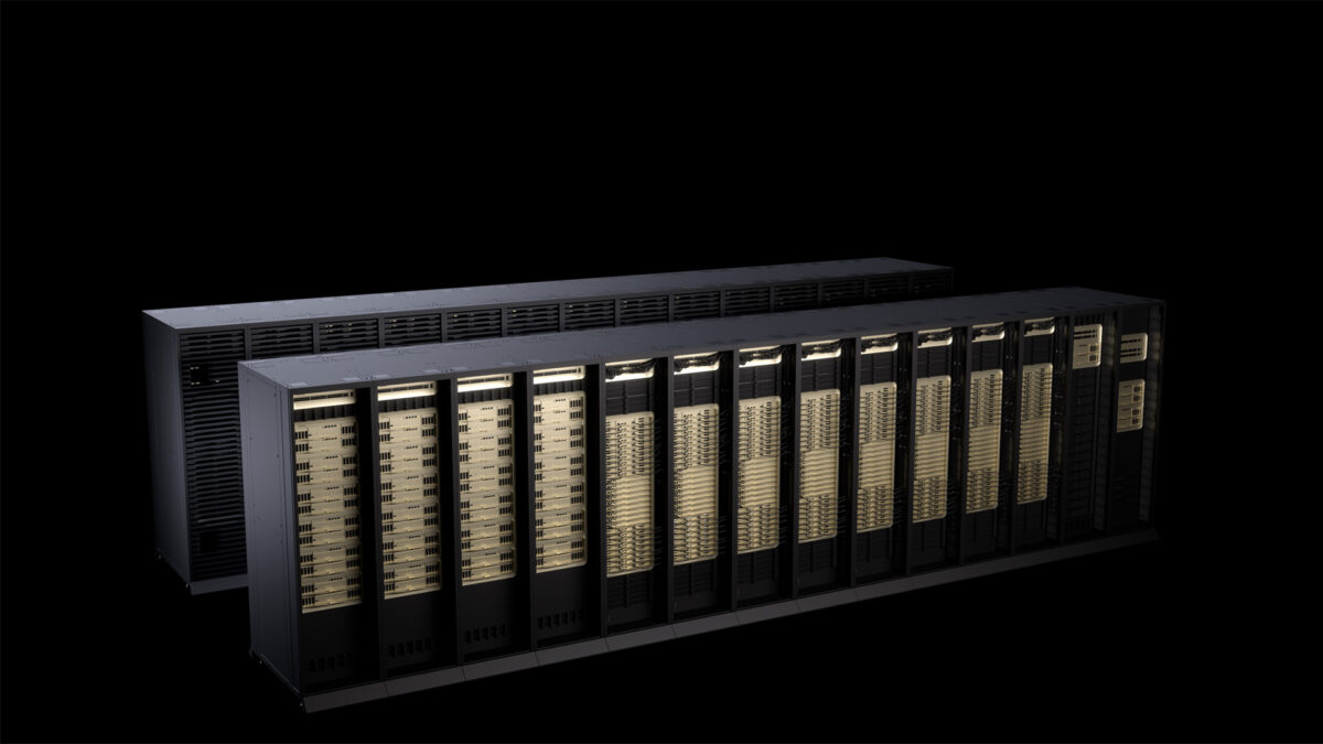
Terafab is a joint semiconductor fabrication venture between Tesla, SpaceX, and xAI, announced by Elon Musk during a livestream from the historic Seaholm Power Plant in Austin, Texas. The name itself — “Tera” referencing a terawatt of annual compute output — signals the scale of ambition. This is not a typical chip packaging facility or design house. Musk is building a fully vertically integrated semiconductor fab that handles every stage of production: chip design, lithography, fabrication, memory production, advanced packaging, and testing, all under one roof.
The facility will be built on the North Campus of Giga Texas, with an estimated investment of $20–25 billion. According to Bloomberg, the initial prototype fab operations will begin in Austin, with small batch production starting later in 2026 and volume ramp-up planned for 2027.
Terafab Chip Factory: Two Chip Types for Earth and Space
The Terafab chip factory will produce two distinct categories of processors, each targeting fundamentally different operating environments:
Edge-Inference Processors (Terrestrial): Optimized for Tesla’s Full Self-Driving software stack, the Cybercab robotaxi fleet, and the Optimus humanoid robot line. These chips are successors to Tesla’s current AI4 silicon, designed for real-time inference at the edge — processing sensor data, making driving decisions, and controlling robotic actuators with minimal latency. Think of them as the brains that let a Tesla navigate a construction zone or an Optimus robot fold laundry.
D3 High-Power Processors (Space-Rated): Radiation-hardened chips custom-designed for orbital AI operations. These D3 processors will power SpaceX satellite constellations, orbital data centers, and xAI’s space-based compute infrastructure. According to Benzinga, Musk stated that roughly 80% of the compute output would go to space deployment, since he believes Earth’s power grid constraints make terrestrial-only deployment impractical at scale.
The 2nm Ambition: Why the Process Node Matters
Terafab is targeting 2-nanometer process technology — the most advanced node currently entering commercial production globally. For context, only TSMC and Samsung are actively working on 2nm production lines, and neither has achieved volume manufacturing yet. Intel’s comparable process (Intel 18A) is still ramping. The fact that Musk is jumping straight to 2nm for a greenfield fab — with no prior semiconductor manufacturing experience across any of his companies — has raised eyebrows across the industry.
The facility plans to start with 100,000 wafer starts per month, eventually scaling to 1 million wafer starts per month at full capacity. At that scale, Terafab would represent roughly 70% of TSMC’s current global output. Musk claims the facility would produce between 100 and 200 billion custom AI and memory chips annually — numbers that, if achieved, would fundamentally reshape the global semiconductor supply chain.
Why Musk Needs His Own Chips — and Why Now
The logic behind Terafab becomes clearer when you look at the numbers. According to Engadget, current semiconductor manufacturers including Samsung, TSMC, and Micron collectively supply only about 2% of the computing capacity that Tesla and SpaceX project needing in the near future. Musk estimates demand for approximately 10 billion robots annually — a figure that, even if wildly optimistic, underscores the scale of silicon required.
There is also a geopolitical dimension. With TSMC concentrated in Taiwan and Samsung in South Korea, both operating in regions with significant geopolitical risk, the case for domestic semiconductor production has never been stronger. The U.S. CHIPS Act has already funneled billions into domestic fab construction (Intel, TSMC Arizona, Samsung Taylor), but Musk is betting that none of these will be enough — or fast enough — for his companies’ needs.
Tesla’s CFO acknowledged to investors that the full Terafab cost — estimated at $20–25 billion — is not yet incorporated into Tesla’s record capital expenditure plan for 2026, which already exceeds $20 billion. This financial detail alone signals how new and unbudgeted this project remains.
The Skeptic’s Case: Can Terafab Actually Work?
For all its ambition, the Terafab chip factory faces enormous challenges that even Musk’s considerable resources may not overcome. Industry experts have been blunt. As New Atlas reported, building a state-of-the-art fabrication facility requires billions of dollars and years of process perfection, skilled workforce assembly, and complex infrastructure development — all described as “astronomically difficult, and quite likely impossible” within Musk’s proposed timeframe.
Consider the precedents. Intel has spent decades and tens of billions trying to maintain leading-edge manufacturing and has still struggled with process delays. TSMC took 30+ years to reach its current position. Samsung’s foundry division, despite massive investment, consistently trails TSMC in yields and customer confidence. The idea that a startup fab — even one backed by Musk’s capital — can leapfrog to 2nm production within a year or two stretches credibility.
Then there is the talent question. Advanced semiconductor manufacturing requires thousands of highly specialized engineers — process engineers, lithography experts, yield engineers, packaging specialists. These people are already in desperately short supply globally. Where will Terafab find them? Poaching from TSMC, Intel, and Samsung is possible but would create its own problems and take years to build institutional knowledge.
Critics, including Electrek, have pointed to Musk’s track record of ambitious announcements followed by delayed or scaled-back execution — the Hyperloop, the affordable Cybertruck, Full Self-Driving’s perpetual “next year” timeline. The concern is not that Musk lacks vision, but that semiconductor manufacturing may be the one domain where vision alone is insufficient.
That said, dismissing Musk entirely would be a mistake. SpaceX proved that vertical integration in aerospace could work against entrenched incumbents. Tesla demonstrated that a startup could scale automotive manufacturing. Whether those lessons translate to semiconductor fabrication — arguably the most complex manufacturing process humans have ever devised — remains the trillion-dollar question.
The Terafab chip factory represents the ultimate test of Musk’s approach: move fast, integrate vertically, iterate aggressively, and bet that speed can compensate for inexperience. The semiconductor industry has never seen anything like it. Whether that is because it is genuinely revolutionary or fundamentally misguided will only become clear when the first wafers come off the line — if they ever do.
Get weekly AI, music, and tech trends delivered to your inbox.
